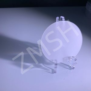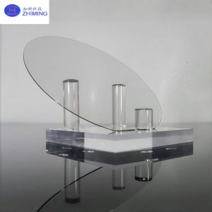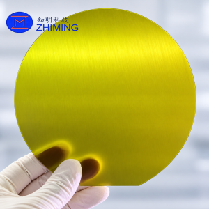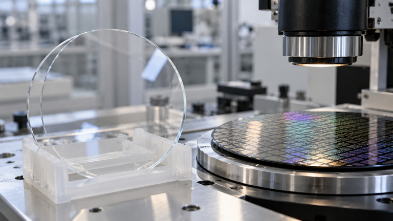
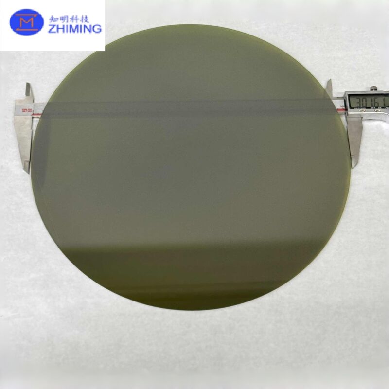
12-Inch 300 mm 4H-SiC Wafer, 750 ± 25 μm
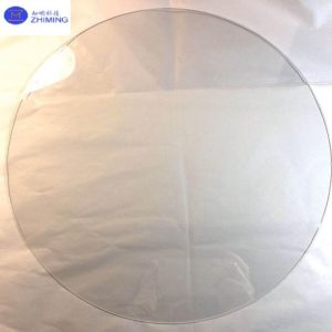
Large-diameter silicon carbide wafer based on the reference listing for 300 mm / 12-inch research-grade substrates. Polytype, conductivity, orientation, thickness, resistivity, defect…
View specifications →Sapphire, silicon carbide, quartz, and specialty materials selected around your device, equipment, and inspection requirements.
Browse by substrate or component family, then confirm the final specification against your process.
Fused quartz plates, precision tubes, rods, boats, and custom process components for semiconductor equipment, thermal systems, and laboratory use.
Browse this familyOptical windows, crystal blanks, ruby rods, watch components, and precision sapphire parts for optical, semiconductor, laser, and industrial applications.
Browse this familySapphire substrates and polished wafers for semiconductor, optical, LED, and research applications.
Browse this familySelected glass, compound, and thermal-management substrates for semiconductor, MEMS, photonics, and advanced packaging projects.
Browse this familySiC substrate formats for power electronics, RF, epitaxy, and device development.
Browse this familyRepresentative products from our substrate and precision-material portfolio.

Large-diameter silicon carbide wafer based on the reference listing for 300 mm / 12-inch research-grade substrates. Polytype, conductivity, orientation, thickness, resistivity, defect…
View specifications →
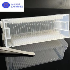
Large-diameter monocrystalline Al2O3 sapphire wafer for LED, optoelectronic, and semiconductor development. Reference listing describes a 12-inch format with DSP/SSP and multiple crystal-plane…
View specifications →
Single-crystal Al2O3 wafer listed for LED, semiconductor, and optical applications. Confirm diameter tolerance, thickness, orientation, polish side, and surface condition against the…
View specifications →
Monocrystalline Al2O3 sapphire wafer for semiconductor and optical development. The reference listing shows a 4-inch C-plane format with double-side or single-side polishing…
View specifications →
High-purity semi-insulating silicon carbide wafer listed in a 4-inch, 350 μm example for AR-glass and semiconductor development. Confirm resistivity, polytype, surface finish,…
View specifications →
Unlike polished or epi-ready substrates, this product does not undergo final grinding, lapping, polishing, or CMP finishing before delivery. The original sliced…
View specifications →Explore how SiC, sapphire, quartz, glass, and thermal-management materials support power devices, RF, optics, process equipment, MEMS, and advanced packaging.
Explore ApplicationsSend dimensions, material, quantity, application, tolerance, and target date for review.
Selection, specification, fabrication, and inspection notes for engineering and procurement teams.

Borosilicate glass remains one of the most useful substrate materials in MEMS manufacturing. While advanced semiconductor packaging has recently increased interest in glass substrates,…
Read article
Choosing between a single-side-polished wafer and a double-side-polished wafer may appear simple, but the decision can have a major influence on semiconductor processing. As…
Read article
The substrate competition behind RF gallium nitride technology is becoming increasingly interesting. In October 2026, Atomera and IQE announced a joint development program targeting…
Read article